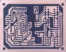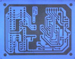
The Artwork
Until recently the artwork had been an area of DIY PCB manufacture which caused the biggest problems. But now by combining high quality laser printing with the Press-n-Peel PCB transfer system these problems have been solved. The first stage is to transfer the circuit layout from the PC to the special Press-n-Peel film. You will find that my projects provide Laser print files (.prn) for printing the circuit layout direct onto this film.
1. I cut the Press-n-Peel film in half for small boards so it lasts longer
2. Put the film in the laser printer so that the print will appear on matt blue side
3. At a DOS command prompt type: copy filename.prn lpt1 to print onto the film
This will produce a contact print where the black image will end up as Copper on the final PCB. Now to transfer the artwork to the Copper board by following the instructions with the Press-n-Peel film.

1. Clean the Copper board very well with the PCB cleaning rubber
2. Heat the cloths iron to 300 deg.F (Acrylic to Polyester setting)
3. Hold the film with the print in contact to the Copper and smoothly iron the film down until the print appears black through the film (about 1min)
4. Allow 5mins to cool down (or speed this up with water) then peel the film off
This should produce a clean black print onto the Copper. If you let the film move or overheat then you will find that the tracks and writing will be smeared and out of focus also the film may be wrinkled up. If you don't use enough heat or heat unevenly then the film may not stick or be dark enough. In either case clean off the PCB and try again, you should get it right after a couple of goes.


4 comments:
Thanks for this valuable information. This gave me an outline idea of making PCBs.
Thanks
Bro where i can Get pcb transfer film....and what cost...
Thanks for the post keep sharing | sqpcb.com
Post a Comment